AD5318 - ADI

The pictures are for reference only, and the specific specifications can be found in the product manual.
Popularity Score
28 points
-
Part NoAD5318
-
ManufacturerADI
-
ChipWorker Part#CW983509030
-
Description2.5V to 5.5V Octal Voltage Output 10Bit DAC in 16-Lead TSSOP
-
DocumentationDatasheet
-
Ships fromMoscow
-
НаличиеIn Stock
-
Estimated PricePrice on Request
Payment Methods and Delivery
{{ estimate }}
Buy AD5318
Stock is limited and changes quickly. Our 24/7 online sales team is ready to respond to your inquiries and orders at any time.
Real stock check
Best price from distributors
Engineer support
AD5318 Global Supplier
| {{ supplierTable.supplier }} | {{ supplierTable.part }} | {{ supplierTable.availability }} | MOQ | {{ supplierTable.delivery_date }} | {{ supplierTable.buy }} | ||||||||||
|---|---|---|---|---|---|---|---|---|---|---|---|---|---|---|---|
|
{{ skuList.vendorName }}
|
{{ noList.partNo }}
{{ strFormat(skuList.part_no) }}
{{ skuList.part_no }}
{{ skuList.mfrEn }}
|
{{ numFormat(skuList.stockQty) }}
{{ search_item }}
|
{{ skuList.moq }} - |
{{ceilNumber(skuList.minDeliveryDay,skuList.maxDeliveryDay)}} {{delivery_date}}
6 {{delivery_date}}
|
{{ formatQuantity(priceList.quantity) }}
{{currencySymbol}}{{ ToEffectiveNum(toDisplay(priceList.price, activeCurrency)) }}
{{viewMore}}
|
|
{{ skuList.vendorName }}
|
{{ skuList.part_no }}
{{ skuList.mfrEn }}
{{ noList.partNo }}
{{ noList.mfr }}
|
{{ numFormat(skuList.stockQty) }}
{{ search_item }}xx
{{ low_stock_text }}
|
1 |
{{weeks_text}}
|
{{ formatQuantity(priceList.quantity) }}
{{currencySymbol}}{{ ToEffectiveNum(toDisplay(priceList.price, activeCurrency)) }}
{{viewMore}}
|
{{price_on_request_text}} | {{currencySymbol}}{{UpToFourDecimals(toDisplay(priceCalc, activeCurrency),skuList.rate)}} |
|
|
{{viewMore}}
|
|||||||||||||||
|
{{viewMore}}
|
|||||||||||||||
|
DigiKey
|
{{noList.partNo}}
{{noList.mfr}}
|
{{ low_stock_text }}
|
1 | {{weeks_text}} | {{price_on_request_text}} | {{currencySymbol}}{{UpToFourDecimals(toDisplay(priceCalc, activeCurrency),1)}} |
|
||||||||
|
Arrow
|
{{noList.partNo}}
{{noList.mfr}}
|
{{ low_stock_text }}
|
1 | {{weeks_text}} | {{price_on_request_text}} | {{currencySymbol}}{{UpToFourDecimals(toDisplay(priceCalc, activeCurrency),0.96)}} |
|
||||||||
|
Mouser
|
{{noList.partNo}}
{{noList.mfr}}
|
{{ low_stock_text }}
|
1 | {{weeks_text}} | {{price_on_request_text}} | {{currencySymbol}}{{UpToFourDecimals(toDisplay(priceCalc, activeCurrency),0.92)}} |
|
||||||||
|
{{submitRFQ}}
|
|||||||||||||||
|
Chipworker
|
{{noList.partNo}}
{{noList.mfr}}
|
{{stockAvailability}}
{{ search_item }}
|
{{moq}} | 1 | 6 - 8 {{delivery_date}} | {{price_on_request_text}} | {{currencySymbol}}{{UpToFourDecimals(toDisplay(priceCalc, activeCurrency),1)}} |
|
|||||||
{{ apiText }}{{ apiTime }}(UTC+8)
Update Data
Chipworker Certification


11+ years sourcing experience
1000+ russia customers
ISO certified supplier
Support small MOQ
*Photos of Our Actual 800 m² Warehouse
AD5318 Specifications
Consulting Engineer >>| Attribute | Attribute Value |
|---|---|
| Part Number | AD5318 |
| Manufacturer | ADI |
| ChipWorker Part# | CW983509030 |
| Documentation | Datasheet |
| expand all | |
| Product Lifecycle Status | Active |
Similar & Replacement Parts
Product Description
- Product Details
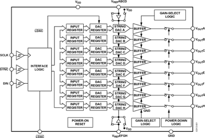
- The AD5308/AD5318/AD5328 are octal 8-, 10-, and 12-bit buffered voltage output DACs in a 16-lead TSSOP. They operate from a single 2.5 V to 5.5 V supply, consuming 0.7 mA typical at 3 V. Their on-chip output amplifiers allow the outputs to swing rail-to-rail with a slew rate of 0.7 V/μs. The AD5308/ AD5318/AD5328 use a versatile 3-wire serial interface that operates at clock rates up to 30 MHz and is compatible with standard SPI, QSPI, MICROWIRE, and DSP interface standards.
- The references for the eight DACs are derived from two reference pins (one per DAC quad). These reference inputs can be configured as buffered, unbuffered, or VDD inputs. The parts incorporate a power-on reset circuit, which ensures that the DAC outputs power up to 0 V and remain there until a valid write to the device takes place. The outputs of all DACs may be updated simultaneously using the asynchronous LDAC input. The parts contain a power-down feature that reduces the current consumption of the devices to 400 nA at 5 V (120 nA at 3 V). The eight channels of the DAC may be powered down individually.
- All three parts are offered in the same pinout, which allows users to select the resolution appropriate for their application without redesigning their circuit board.
- **Applications**
- Portable battery-powered instruments
- Digital gain and offset adjustment
- Programmable voltage and current sources
- Optical networking
- Automatic test equipment
- Mobile communications
- Programmable attenuators
- Industrial process control
- ### Features and Benefits
- AD5308: 8 buffered 8-bit DACs in 16-lead TSSOP A version: ±1 LSB INL, B version: ±0.75 LSB INL
- AD5318: 8 buffered 10-bit DACs in 16-lead TSSOP A version: ±4 LSB INL, B version: ±3 LSB INL
- AD5328: 8 buffered 12-bit DACs in 16-lead TSSOP A version: ±16 LSB INL, B version: ±12 LSB INL
- Low power operation: 0.7 mA @ 3 V
- Power-down to 120 nA @ 3 V, 400 nA @ 5 V
- Double-buffered input logic
- Guaranteed monotonic by design over all codes
- Buffered/unbuffered/VDD reference input options
- Output range: 0 V to VREF or 0 V to 2 VREF
- Power-on reset to 0 V
- Programmability
- Individual channel power-down
- Simultaneous update of outputs (LDAC)
- Low power, SPI-®, QSPI-™, MICROWIRE-™, and DSP-compatible 3-wire serial interface
Delivery
Ordering Information
-
These terms and conditions are for reference only. The actual terms and conditions are subject to the sales staff's quotation.
- Please check the technical specifications of the products when ordering.
- MOQ is the minimum order quantity required to purchase each part.
- If you have special ordering instructions, please indicate them on the order page.
- Pre-Shipment Inspection (PSI) will be used when ordering.
- You can check the status of your order in the “My Order” section of your personal account.
- Orders cannot be canceled after the package has been shipped. View more > -
- Works with both individual and corporate clients. View more >
- All prices on the website include 22% VAT.
- Invoices are issued in the currency specified, but payment is made in Russian rubles at the exchange rate on the day of payment.
- If you need a detailed invoice or a tax identifier, please contact us. -
- Delivery will take between 1 to 2 weeks after the shipment is sent to your country.
- Your order will be processed only after the invoice has been paid.
- The tracking number will be sent to you after the order is shipped. (It may take up to 24 hours for the information to be available from the carrier.) View more > - - Carefully tested and packaged by ChipWorker- Vacuum packed - Anti-static packaging - Anti-vibration foam
-
- Income quality control (IQC), 800+ qualified distributors.
- Authorities test the chip to ensure the quality, authenticity and safety of your device.
- Decapsulation control
- X-ray inspection
- XRF inspection
- Electrical testing
- Surface testing
Contact Us
Contact us today and a sales representative will provide you with a quote for any model.
 Customer Service, Quick Links
Find immediate assistance and access to our most used services through our Quick Links. Your satisfaction is our priority.

